-
Will Langford authoredWill Langford authored

Pulse Generator Design
The Waveform
I've had some email correspondance with Jaako Fagerlund (who is one of the few people who has made his own desktop EDM) and he had a really nice explanation of how the waveform should work:

The waveform is quite simplified in that picture, but it explains the basics very well. Looking at the upper graph you see gap voltage versus time. As the voltage is switched on, the voltage in the gap is the same as the generators output. If the gap is small enough, the dielectric breaks down and a spark is ignited. This plasma channel is of course lower resistance, so now current (lower graph) starts to flow. The gap voltage drops to basically what the plasma channels resistance times current is. In the graph this area is the lower voltage after full (open) voltage. Then after the on time pulse length is achieved, the generator switches of, the current flow stops and the gap voltage is zero until the generator once again applies a new pulse.
Based on this, this is the basic circuit schematic that I'm after:

With a few more details filled in:

My understanding of the waveform:

References:
Parts:
-
Hearty N-Type MOSFETs: IRFP460A FDB20N50F SDB45N40 (least R_dson)
-
High-side gate drivers:
LM5107 UCC27200AI could get away with just using one of these (and using a low-side mosfet to do the discharge control). The problem with this is that then the workpiece and worktable are at high voltages whenever the machine is on. So I suspect I'll go with two…- It turns out that these don't have integrated charge pumps and so don't work unless the source of the FET is routinely grounded.
- The LTC7001 seems like a good option to replace these
- diode for fast recovery may be useful for high frequency operation
-
Capacitor: 6.8uF conductive polymer
-
window comparator
-
Current sense amplifier: LTC6101
- Sense resistor: 4mOhm, 3W
Timing Calculations
from: https://www.vishay.com/docs/73217/an608a.pdf
Effective Resistance seen by the gate driver: $ R_G = R_g + R_{gext} $
Effective capacitance seen by the gate driver: C_{iss} = C_{gs} + C_{gd}
switching time: $ t = R_G C_{iss} \times \ln{\frac{1}{1-V_{gs}/V_{GS}}} $
Design Decisions
I decided to focus the first revision of this board around the idea of doing as much as possible in firmware on a microcontroller rather than as a static implementation in hardware.
After much flipping back and forth between datasheets, digikey tables, and eagle libraries, I eventually ended up at this board:

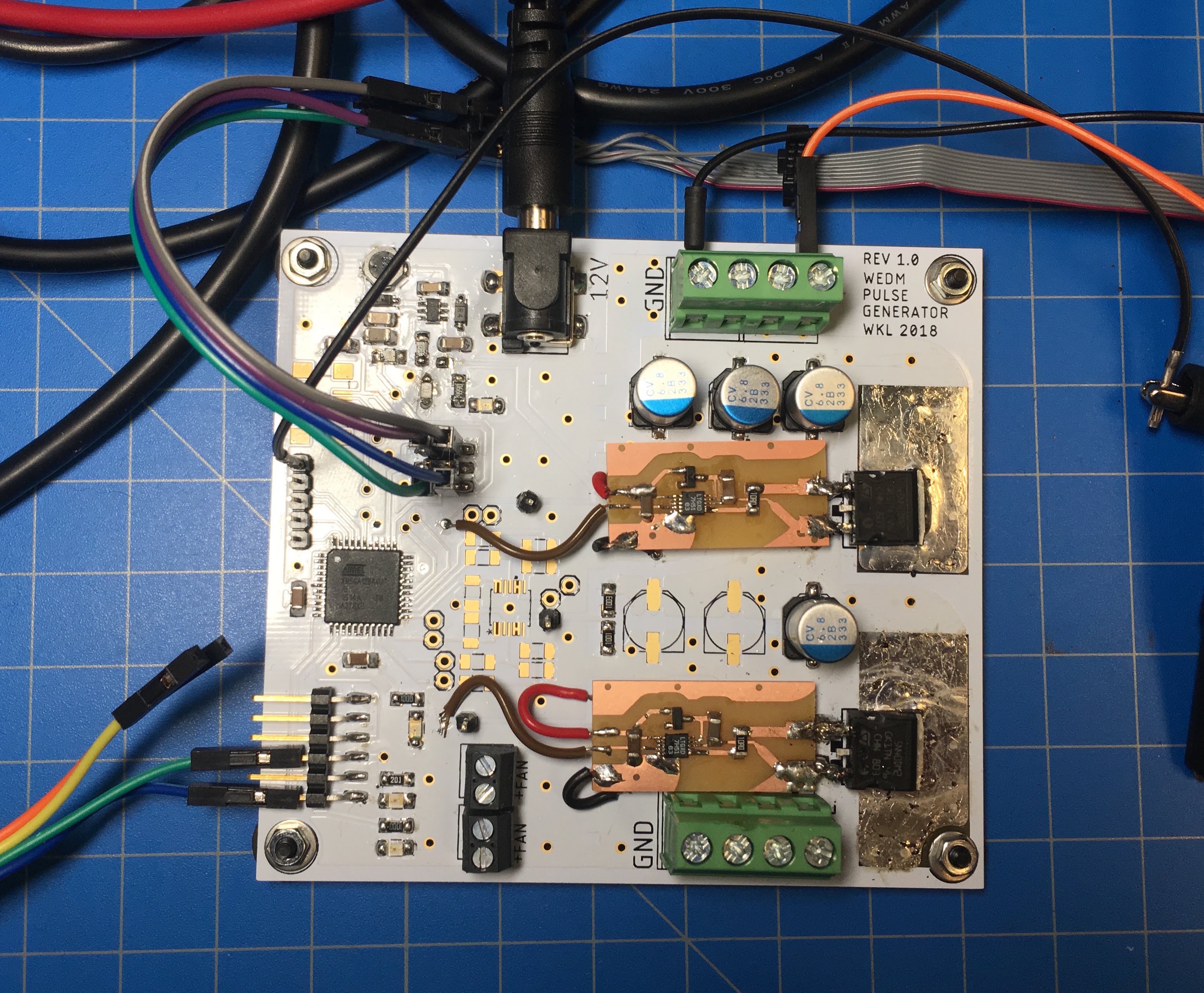
I've more-or-less tried to keep the board layout pretty divided based on function. This will hopefully help with debugging and I believe is also good design practice when dealing with mixed signals (both digital/analog and high-power/low-power).
All of the high-current/high-voltage things are on the right side of the board. This includes the two power MOSFETs (SDB45N40), two banks of low ESR capacitors (6.8uF conductive polymer), as well as the high-side gate drivers (LM5107). 100V DC power comes in at the top of the board, which will likely just be supplied by a bench top 100V supply initially (although, ultimately I may take mains power in and use a bridge rectifier to get that voltage).


On the opposite side of the board are all of the small-signal computing and communication peripherals. I decided to use an xmega128a4u as the main processor. I chose this over other options (including the NRF52, ATSAMD21, ATSAMD51, ATmega32u4) for it's speed and ease of timing. After talking with Sam and Jake, the ATSAM architectures just seemed a little unnecessarily complex for this dedicated controller. Some of the notable features of this XMega include a 2 Msps analag to digital converter (which may just be fast enough to directly sample my ~50KHz pulses), two built-in analog comparators, and all of the necessary PWM/timing peripherals. Because I had space, I included both USB and FTDI communication channels (since I've never tried getting USB going on an XMega before). I also broke out a few extra GPIO/ADC pins… just in case...


Connecting those two regions, is the sensing and control circuitry. This region needs to be able to sense the voltage levels of the spark and filter capacitors relay information to the microcontroller to decide whether to turn on or off the high-power MOSFETs. I'm using a 4-channel comparator wired as a dual window-comparator. This will let me set desired voltage windows (across the spark capacitors) that I can then modulate the MOSFETs to achieve. I plan to produce the variable voltages by low-pass filtering PWM signals from the microcontroller. This is just one idea I have for implementing this kind of control and I intentionally left my options open for experimenting.


The Assembled Board:

Errata
- need to tie unused low input pins of the gate drivers to ground (should be easy to bridge)
- need to jumper between HS pin of the gate driver and MOSFET source (bottom of mosfet)
- should use switch instead of solder jumper to switch between 5V and 12V (or better yet, have it automatically switch to the higher voltage source… I can probably do this with properly rated shottky diodes)
- I don't have the overhad to use a normal 0.7V diode with the 5V supply.
Something called an ideal diode works for this though.But this doesn't work above a 6V reverse voltage. - This one would likely scrape by for the 5V side (0.5V drop at 500mA). (actually this one would work, but I think the BAT54S 200mA schottky diode in the fablab inventory would work was well. It has a higher 800mV drop at 100mA but the MCP switching regulator should be okay down to 4V)
- Here's a diode for the 12V side, which I may not even need.
- I don't have the overhad to use a normal 0.7V diode with the 5V supply.
- should have pull downs on both inputs to gate drivers and inputs to mosfets (for safety)
- unclear if I need higher powe-rated resistors for the gate drive resistor. They'll be undergoing high momentary currents but their average power dissipation is well below their 1/4W rating.
Gate Driver Replacement: LTC7001
It turns out that I picked a gate driver that didn't have an internal charge pump and so relied on the source of the high-side MOSFETs being routinely grounded in order to establish charge on the bootstrap capacitor. My work to discovere this is here now: Debugging Gate Driver
Anyway, I picked a new gate driver with an integrated charge pump (see parts list above).
In order to test this out without sending out for an entirely new board, I will redesign the board and then crop and mill pcbs to replace the small sections that are different than before. This should let me desolder the present boards and lay these new components right on top.
from the datasheet I should:
- Use a bootstrap capacitor of at least 0.56uF (\frac{10 Q_g}{1\text{V}}) (let's start with 1uF)
- Use an external diode for faster recovery.
- Include space for gate resistor (although the pull-down and pull-up FET's in the gate driver have 1ohm and 2.2ohm R_dson respectively).
Here's what the board section looks like. The circuit doesn't require much. There's two 1uF capacitors: one which serves as the boost capacitor and one simply acts as a bypass between Vcc and ground. A resistor in series with the gate will let me limit in-rush current. Two 1nF capacitors are pictured at the output as a simulated capacitive load.

I tested the gate driving circuitry independently to verify that it was working as expected. Here it is taking the 2.5Vpp square wave from the AFG on my scope and boostin it up to 12Vpp (even with a 7V DC offset). The rise time for a 1nF load (with no series resistance) is about 12ns and is about 20ns for a 2nF load. I expect the gate of the MOSFET to be ~3nF so I should expect in the ballpark of 30ns rise time.


Once I integrated the gate-driver circuitry to the main pulse generator board, I found that the board was not bootstrapping the voltage. At one point I was also getting no output from the discharge gate driver and so I suspect I fried it. I replaced it and the charge gate driver and added a 10ohm resistor in series with the gate to limit the inrush current. So far, I this seems to have helped.


To try to debug the bootstrapping voltage, I replaced the 1uF bootstrap capacitor with a 33uF one (rated for 25V). This slowed the decay of the output voltage but it still ultimately stopped working after a few seconds. This led me to suspect I was operating at too high of a frequency. By decreasing frequency I was able to stabilize the voltage. It's stable at 488Hz, but not at 3.9KHz (there's no in-between with the way the counters are currently setup). At this frequency, it it able to be PWM'd down to 6/1024 (0.5%) while maintaining 12V across gate (and it's very unlikely I'll need duty cycles below that).
This 500Hz is normally limited, I believe, by the current (30uA) the integrated charge pump uses to refill the boostrap capacitor. With a gate charge of 56nC, 30uA equates to 535Hz. Theoretically, an external diode is supposed to help for switches at higher frequencies than this. When TS is less than 12V, it's clear that the diode greatly reduces the time BST takes to get to 12V. But when TS is consistenly above 12V, it seems like D1 would always be reversed biased and wouldn't contribute to the time it takes to refill the capacitor. From the datasheet...

So, it's unclear to me if I'd be able to get above this ~500Hz limit with the integrated charge pump. An alternative solution could be to build my own dedicated external charge pump.
Moving on… With both gate drivers working, I tested pulse output with a 10ohm load (a through-hole resistor placed between the output and ground). The pulses look good:

I then replaced the resistor with a spark gap. For testing I'm just using a bullet connector as the workpiece and the lead of a through-hole resistor as the tool. I initially tried having the workpiece grounded and the tool hot, but found it was much more favorable the other way. I would like to know more about the theory behind this. I guess part of it must be that the electrons (or ions?) are moving from ground to hot and so the workpiece should be hot….?

Here's what the pulses look like when they're making sparks:


I'm using a 20V source with a current limit of 500mA (although the circuit is not drawing more than ~60mA even when short circuiting). The pulses look more or less like I'd expect. The blue trace is connected directly to the hot end of the pulse output and the yellow is connected to the voltage divider spanning the spark capacitor bank. The pulses start at the full 20V, then once the sparking starts, it drops to ~10V in the picture on the right. The capacitor then starts discharging at a rate controlled by the RC constant (R_gap and C_spark, which is currently 6.8uF). When the workpiece gets too close to the tool, it short circuits and the spark capacitor's voltage drops all the way to zero.
It's nice to see that the voltage divider output of the spark capacitors gives a good indication of how the cut is going. It maps exactly (100:1) with the shape of the output waveform. The negative transient as the pulse is stopped is something that I might want to pay attention to as something that could potentially damage the ADC.
Here's what the sparking looks like:

And here's the hole I made… The cut is remarkably asymmetric; the tool (resistor lead) had som surface damage but remained largely in tact while a significant amount of the the workpiece (bullet connector) was worn away:


I also did a test with a brass GIK and another bullet connector (this was before I figured out the right polarity so the bullet connector took way to damage than the GIK part):


Next Steps:
-
figure out how to increase frequency
- I think this will likely involve an auxillary charge pump
- Try a smaller capacitor… this should get initially charged much faster and as long as it has enough charge to switch the MOSFET, it should be no different than a big hefty capacitor.
- according to the datasheet, they're theoretically capable of getting 20kHz PWM using a 15nC transistor (4x less gate charge than mine)… but that's 4x, not 40x so I'm a little confused still. This transistor would probably work for me given that I likely over-spec'd the one I originally picked.
- or... I could switch to P-channel MOSFET's and save having to do all of this charge pumping.
- this one is pretty good: P-channel 150V, 300W, 55nC or 100V, 60nC, 50W
- these can be driven with a relatively simple level shifter circuit
-
try higher power (test 2x 50V supply)
- put it in the case for >50V
-
start working on control:
- sample VC (with ADC) in realtime and see how clear a signal I get (at 500Hz, I'd expect it to be pretty good with ~2Msps)… Zoomed out on the scope, I can see the pulses quite clearly even at only 100Ksps.
- start with just having this give an output to tell me to turn the adjustment screw or not
- make a stepper motor board and connect the two together (maybe with an opto-isolated serial connection?)
- or… just use the tabletop instron… or better yet, the Desktop EDM!
-
pretty soon I'm also going to have to start worrying about a constant source or clean DI water. For these little tests I can just squirt some in a beaker but that won't work for long given how hazy the water gets after just a few minutes of constant burning.
-
After frying another gate driver (the discharge one) during testing, it seems like the circuit could use a little more protection. I may need to include negative voltage protection on the source of the MOSFET's
- like this: (from http://www.ti.com/lit/ml/slua618/slua618.pdf)
- this one looks good: DFLS1150

PMOS Re-Design?
- NMOSFET to drive PMOS gate: 3.3v logic compatible and Vds up to 100V
After simulating a P-MOS circuit, I'm finding that there's an excessive amount of loss in the level shifting circuit. In order to switch the gate as quickly as I would like, I found that those resistors need to be on the order of 1kohm (or less). With a 100V supply, this is ~10W of dissipation whenever I want to open the gate. Not ideal...
There may be a way around this with totem-pole drivers but I haven't wrapped my head around that yet.
This got me back to thinking whether I could just provide my own charge-pumped boost voltage to the gate driver so I don't have to rely on it's little trickle of current. I simulated a 555 version of this but am finding that I get the same problem that I was having with the bootstrap circuits: the capacitor who
this appears to be one way to do it... but it confuses me
or do a radical redesign with logic level high voltage mosfets
like this: NTP60N06L (60V, 60Amp, Vgth = 1.5V)
This guy appears to be asking the same question I am. This is the circuit he came up with:

or use isolated dc/dc converter....? (idea from here)