## UCBus Stepper Driver Log
### Notes for Next Rev
**2021 01 11**
- add endstop option pinout
- build with encoder placed,
- choose sense R for more current potential
- try to make SPI lines to encoder cleaner: these can go ~ 20MHz
- fix the jtag pinout
**2020 10 06**
Consider doing a *very* simple version of this that is D21, A4954 dual h-bridge, AS5047 (option), no crystals, etc...
**2020 09 21**
Have these back, am testing. Have a JTAG pinout error, obviously didn't check very well. 3v3 and GND connect at the header - not cool. Only when plugged in is this an issue, I think I can just remove a pin...
Oh lawd, that works, godbless the hotfix.
**2020 08 18**
I'd like to make a dedicated step board, there will be many of these. I should follow the existing pinout. Would like to:
- flip it, side mount LEDs (find clk and err lines that will match later module revision) and reset button pinch
- heatsink on the flip
- AS5047P on the IC side
- debug on 'top' flipped side, if space, else use module type to debug
- add temp sensor RTD
- smaller sense resistors, spec to go full-er width at 3v3, currently only does 1.6A or so?
- does a slightly different A4950 exist with OCP / Temp Shutdown pin exist?
- still some observable oddball stepper behaviour: when turnt on, then left, eventually you might hear some clicking / see motors draw less current, then spike back up. I would guess at a DAC refresh issue, but am not sure.
- might want / probably do want the hold-down shrouds for IDCs
For JTAG: just do 'lock' 2x5 0.050" header, don't have to solder, can use straight header once for debug, solder on if flashing more often. Less BOM cheaper PNP.
**2020 07 27**
- A4950 lower / heat pad: bigger holes to hand solder thru, or / and exposed flags on top to see that wicking has happened
- 0.2 ohm sense resistor means maximum current per channel is 1.65A, this is OK, things get hot around there, could be nice to have more headroom.
## Components (roughly!)
| Part | PN |
| --- | --- |
| 2x5 Shrouded | ED1543-ND |
| A4950 | 620-1400-1-ND |
| Cap 150uF 35v SMD 6.6mm | 565-5148-1-ND |
| TVS Diode | SMAJ30ALFDKR-ND |
| 2010 Current Sense Resistor, 0.2Ohm 1W | do 0.1Ohm now |
| 1206 10uF 35v Ceramic Cap | GMK316BJ106KL-T |
| 0805 0.1uF 35v Ceramic Cap | C0805C104Z5VACTU |
| 0805 120R | CRGCQ0805F120R |
| 0805 1k | RC0805JR-071KL |
| 0805 10k | RC0805FR-0710KL |
| Screw Terminal 3.5mm Pitch | 277-1860-ND |
| Side Headers (Debug) | 1849-PM20206HBNN-ND |
| Part | PN |
| --- | --- |
| LED Side Mount 0603 Green | 160-1478-1-ND |
| Red | 160-1479-1-ND |
| Yellow | 160-1480-1-ND |
| Right Angle Reset | P16767CT-ND |
| Latching Shrouded Connector | 71918-210LF |
| Big DIP | 219-8LPSTRF |
| 0805 22uF 35v | 445-14428-1-ND |
| 0.1 Ohm Sense R 1W 1206 | P.10AUCT-ND |
| Side Reset | EVQ-P7J01P |
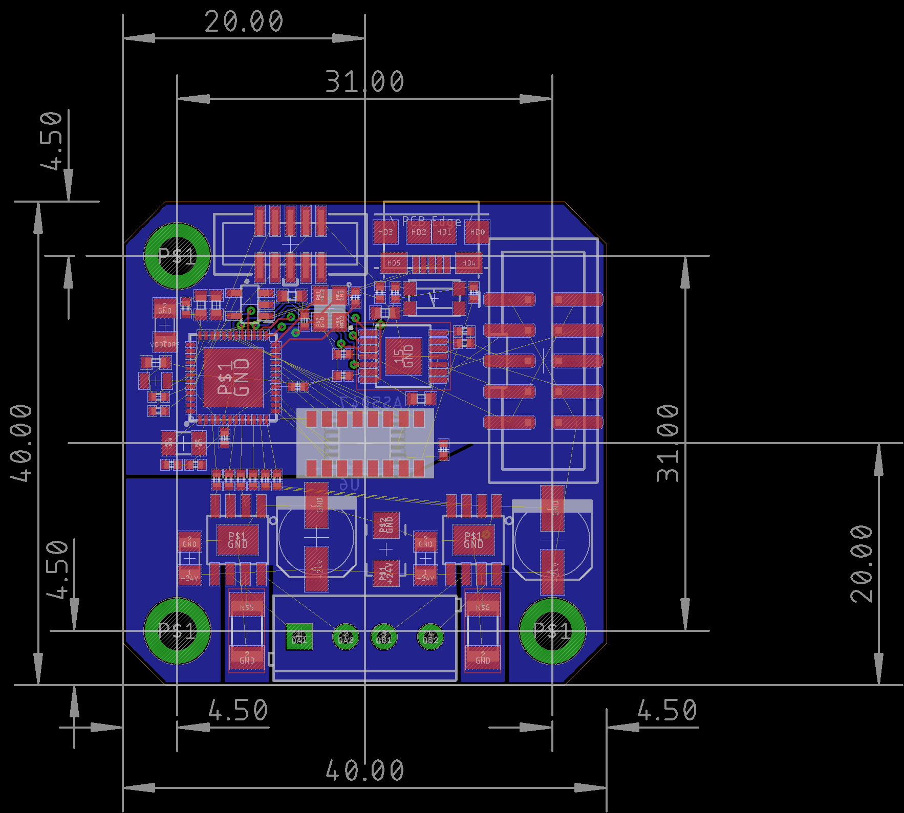
## 2021 01 13
Ordering a handful more of these, so I'm adding an endstop pin.
Deltas are:
- add endstop pin
- spec 100mOhm sense r, not 0.2 as previous
- spec place for AS5047P
- fixed the jtag pinout
## 2020 08 20
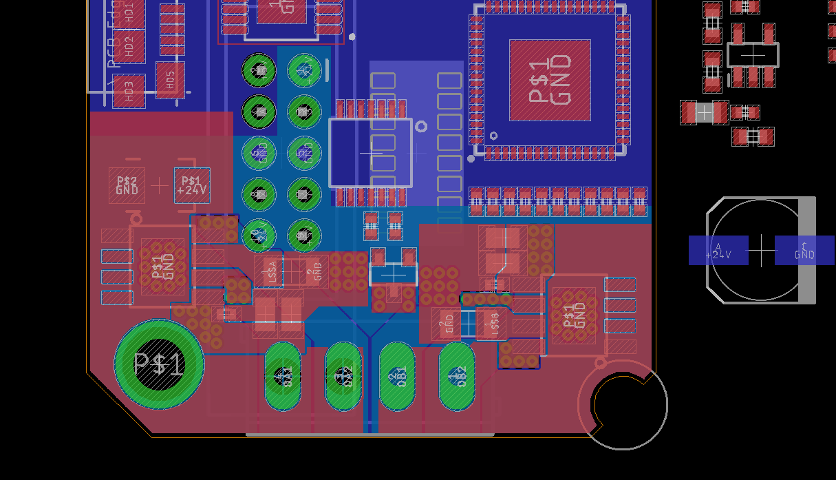
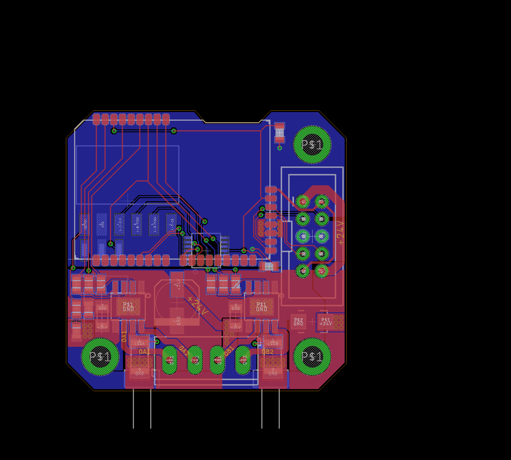
I'm getting into a redesign for these, going to melt the module circuit on board and try to fit it to an N14 footprint.
OK, I think the schematic is there, now I just need to adjust the sense R value, add a temperature sensor, and expand the shroud document for clips... Then I'm into the routing adventure. The A5950 exists, which is bigger / fancier than the A4950, but slightly smaller current. It has a different interface (not greatly) and can report thermal events / other faults... It also has an analog sense output, for the cases where I might want to actually read the top of the sense resistor. Probably this isn't worth it for now, I'll continue with the A4950. It works.
Can get away with a 1206 1W sense resistor, rad.
This is going to be a pain, it's pinched.
Also, the DIP switch... won't be accessible from the top. Yikes. I could eat it, and setup DIPs before they go down, or I could solder it on top manually, getting a bigger component to make that easier. This is the only real full stop issue... and it also saves some space.
Yikes. Yeah, I guess DIPs on the rear are the move. Maybe eventually the bus protocol becomes mature enough to support auto-config at startup and then EEPROM / Flash memory allows local storage of 'drop #' configuration from the UI. For now, whatever, solder on top.
To route, my biggest Q is about the motor side routing: nice GND paths for sense Rs, big traces out to motors. Heat. I think I am working this out OK... I also need to ground the bottom of the power caps... Did that through the same GND vias as the sense R is pulling from. And finally, some big GND heat-spreaders on top...
For thermal measurement, then, I would properly put two RTD sensors on, one for each bridge. The bridges are separated by about 20mm, not sure how long it would take a heat up to spread between the two, but I guess it's short enough, I'll just tap the center with one RTD. Not even using this yet, so... that's fine.
That's enough for tonight! Tomorrow I am hopeful I can get through the micro support etc and the actual business. But these polygons feel good.
## 2020 08 21
Lettuce see if this can go complete today, and ... BOMs out as well? The dream.

I'm feeling generally unorganized with this. The IDC really crash lands right in the middle of everything. Maybe these things are just messy.
Alright, tucking the RS485 driver up a little makes me feel better about the thing aesthetically, which anyways is whatever. I think it's about fine, I'll get into routing.
Woof, the *monster* DIP and the latching connector alone really claim the whole back side of this thing.
Routing... I think I'll do the power side first.
It's just occurred to me that the DIP switch will prevent solid heat sinking on the bottom layer. That's a shame but I guess it'll be impetus to eliminate the need for DIPs. If I'm not careful this thing is really going to F my monolithic GND as well.
OK, wowowee... just routing power now. Thing is a nightmare, I hope I haven't set up any gnd loops or othery mayhem...
I am just nearly through this, have to route out one last piece of the 24v net, then do checks etc.
Damn, I have also just seen that the screw terminals can't be mounted when a latched IDC is used. I'm OK with this, prefer to solder motor leads on directly anyways, but it'd be better to have the terminals... I think that's just going to have to be OK. Sorry everyone.
Well, it passes the DRC. I've made all of the adjustments. I think it's just BOM and MacroFab then.
## 2020 08 12
I have a smoothieware port running inside of these, here it is making steps. Next is connecting that to a browser to send paths, then syncing smoothie instances across motors via the ucbus.

## 2020 07 28
### DAC MicroStepping
So, moving to microstepping actually should be kind of fun. Generate a sine table, do current *in divs of that* to avoid awkward scalings of the table, then make DAC writes on some steps, pin inversions when crossing zero markings at 2, 4, 6, 8, etc. Party on.
```cpp
// sequence like
// S: 1 2 3 4 5 6 7 8
// A: ^ ^ ^ x v v v x
// B: ^ x v v v x ^ ^
```
So... I want a sine table, then to increment through that table at each 'step' and when I hit a zero crossing, flip bits. I can start coils 90' out of phase, and just step together.
I'd be totally fine with 1/16 microstepping, I'll write a table for 256 steps and can change the increment step to adjust.
Great, I've this doing 256 microsteps, the code is pretty similar, but looking from a LUT and tracking position within that table.
```cpp
// sine, 0-1022 (511 center / 'zero'), 256 steps
uint16_t LUT[256] = {
511,524,536,549,561,574,586,598,611,623,635,647,659,671,683,695,
707,718,729,741,752,763,774,784,795,805,815,825,835,845,854,863,
872,881,890,898,906,914,921,929,936,943,949,956,962,967,973,978,
983,988,992,996,1000,1003,1007,1010,1012,1014,1016,1018,1020,1021,1021,1022,
1022,1022,1021,1021,1020,1018,1016,1014,1012,1010,1007,1003,1000,996,992,988,
983,978,973,967,962,956,949,943,936,929,921,914,906,898,890,881,
872,863,854,845,835,825,815,805,795,784,774,763,752,741,729,718,
707,695,683,671,659,647,635,623,611,598,586,574,561,549,536,524,
511,498,486,473,461,448,436,424,411,399,387,375,363,351,339,327,
315,304,293,281,270,259,248,238,227,217,207,197,187,177,168,159,
150,141,132,124,116,108,101,93,86,79,73,66,60,55,49,44,
39,34,30,26,22,19,15,12,10,8,6,4,2,1,1,0,
0,0,1,1,2,4,6,8,10,12,15,19,22,26,30,34,
39,44,49,55,60,66,73,79,86,93,101,108,116,124,132,141,
150,159,168,177,187,197,207,217,227,238,248,259,270,281,293,304,
315,327,339,351,363,375,387,399,411,424,436,448,461,473,486,498,
};
```
From that sine table, which has zero around 511 (is 0-1022 full swing), I rectify a DAC output table - I can also change C_SCALE here to adjust current.
```cpp
void STEP_A4950::init(){
// all of 'em, outputs
AIN1_PORT.DIRSET.reg = AIN1_BM;
AIN2_PORT.DIRSET.reg = AIN2_BM;
BIN1_PORT.DIRSET.reg = BIN1_BM;
BIN2_PORT.DIRSET.reg = BIN2_BM;
// transform full sine table for DAC table
// i.e. rectify...
for(uint16_t i = 0; i < 256; i ++){
if(LUT[i] > 511){
dacLUT[i] = (LUT[i] - 511) * C_SCALE;
} else if (LUT[i] < 511){
dacLUT[i] = abs(511 - LUT[i]) * C_SCALE;
} else {
dacLUT[i] = 0;
}
}
// start condition,
step();
}
```
```cpp
void STEP_A4950::step(void){
// increment: wrapping comes for free with uint8_t
if(_dir){
_aStep ++;
_bStep ++;
} else {
_aStep --;
_bStep --;
}
// a phase,
if(LUT[_aStep] > 511){
A_UP;
} else if (LUT[_aStep] < 511){
A_DOWN;
} else {
A_OFF;
}
// a DAC
dacs->writeDac0(dacLUT[_aStep]);
// b phase,
if(LUT[_bStep] > 511){
B_UP;
} else if (LUT[_bStep] < 511){
B_DOWN;
} else {
B_OFF;
}
// b DAC
dacs->writeDac1(dacLUT[_bStep]);
}
```
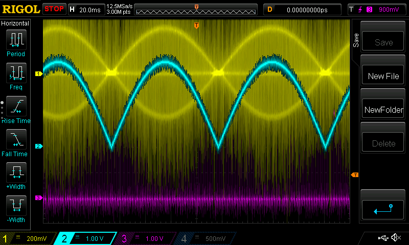

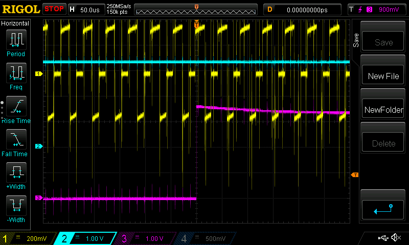
These are zooms of the same setup: pink channel is the step increment (on edge), blue is the DAC output going to the VREF on the A4950, and the yellow traces are direct readings from the top of the sense resistor on that A4950. Seems like a good amount of current is flowing back into GND, which is kid of interesting - I'm always amazed when I look at traces like this how messy things actually get. Also - you'll see this super noise everywhere, I'm pretty sure that's coming out of the PSU, next time I roll a PSU base-board, I'll try to add the right scale bypass caps to clip these high frequency pulses out.
So, that's it for low level stepping code, next I'm going one layer up to motion control - thinking now that acceleration should be planned at each motor - if they all run the same algorithm, and clocks are synced over the bus, I should be able to expect them to work together. This way, I won't have the awkward / unavoidable condition where some step moves (in execution time) are necessarily longer 'on the wire' (in transmission time) which will *eventually* starve some buffers, somewhere, for sure - this is only a problem if I transmit some high-speed move, motors are ripping along, and then starve the buffers before the decelerating moves arrive: crash, inductive spikes, bad times all around.
## 2020 07 27
OK, this morning I soldered up 4 stepper boards, and tested loading the bootloader onto one (it worked, bless). For the week, I'm sort of focused on these circuits while also trying to finish the Clank-LZ cad / spec to hand off - that's waiting on prints. So I guess I should just get to it and start in on new HW drivers for these things.
### DAC Setup
First task is the DAC setup. I didn't put any manual AREF config in for the A4950 so the stepper success is riding on this. Now! I could just do the arduino IDE for this... That works, took zero register banging. Should probably just proceed until this becomes limiting, it's about 1.5 or 3us to write, surely it could be faster but I likely won't need it to be until I want to stream some hella music bitrates or something like that.
I should do the clock / error lights as well.
oof. I done goofed and didn't route the error or clock lights back to the micro. oy. glad it's non-halting, but damn those are important to have.
Well, guess I should just try to step. Will set AREF on the A4950s to... 1/6 of total? Sure. Setting all low to be in braking mode, and I'll see about connecting the thing to power to see if it explodes or not. Wish me luck.
OK, didn't blow up. I've it holding, I think I'll check those vsense lines. It would appear that only my B Hbridge is currently driving current.
So, strangely, the DAC1 I can write once and it stays at the set level, when I write to DAC0, it 'fades' if I don't continue to write. I'm looking at some register banging to avoid this, might have to abandon the arduino quickfix and do these properly, my guess is that they are doing something strange to turn on the DAC, resulting in this. Yeah, based on the fact that when I swap the order that I call the DAC-write in, this behaviour changes pins, I actually need to get down to brass tracks here and write my own DAC register code.
Well, I can get the DACs running, and I've reduced the call from 1.5 or 3us towards 100ns (up to 1us, rarely). However, I can't get them to rest - they have to be periodically refreshed. That's fine for now.
I can move on now to moving some step trains along, and eventually perhaps I'll be up to 'microstepping' - then I can proceed with real motion control. I'll do that by implementing ... most ? of smoothieware on one step board, and then afterwards determine what's best-case to distribute its execution across boards, either splitting planner | block executioners, or nestling one whole smoothie roll in each motor, matching configs, and bussing clocks and motion grams.
### Step Sequencing
OK, so I'll have a step timer, I can put the DAC refresh in there, no worries. For now, I want to see about checking (again) that my HBridges will both HBridge, and then generate a little open loop, full current step train. From there, I can think about microstepping.
Finishing this segment of work would mean having clean step(); and dir(b); functions that I can call from whatever step timer ISR I end up implementing. Microstepping would be cool, but at this point I'll take the 400 from half stepping that I can accomplish w/o any sin tables.
Alright, I've that working - no sin tables, and w/o even half stepping, it's *clanky* as in, not very smooth at all no no. OK, now with half steps it feels better. And I think I am building an understanding of how this becomes a micro-stepping driver... and maybe even the fully closed-loop getdown seems a reasonable task. That's some kind of progress.
For the log, here's the ref:
```cpp
// pins to A4950
#define AIN1_HI AIN1_PORT.OUTSET.reg = AIN1_BM
#define AIN1_LO AIN1_PORT.OUTCLR.reg = AIN1_BM
#define AIN2_HI AIN2_PORT.OUTSET.reg = AIN2_BM
#define AIN2_LO AIN2_PORT.OUTCLR.reg = AIN2_BM
#define BIN1_HI BIN1_PORT.OUTSET.reg = BIN1_BM
#define BIN1_LO BIN1_PORT.OUTCLR.reg = BIN1_BM
#define BIN2_HI BIN2_PORT.OUTSET.reg = BIN2_BM
#define BIN2_LO BIN2_PORT.OUTCLR.reg = BIN2_BM
// set a phase up or down direction
// transition low first, avoid brake condition for however many ns
#define A_UP AIN2_LO; AIN1_HI
#define A_OFF AIN2_LO; AIN1_LO
#define A_DOWN AIN1_LO; AIN2_HI
#define B_UP BIN2_LO; BIN1_HI
#define B_OFF BIN2_LO; BIN1_LO
#define B_DOWN BIN1_LO; BIN2_HI
// sequence like
// S: 1 2 3 4 5 6 7 8
// A: ^ ^ ^ x v v v x
// B: ^ x v v v x ^ ^
void STEP_A4950::step(void){
if(_dir){
_state ++;
if(_state > 8){ _state = 1; }
} else {
_state --;
if(_state < 1){ _state = 8; }
}
switch(_state){
case 1:
A_UP;
B_UP;
break;
case 2:
A_UP;
B_OFF;
break;
case 3:
A_UP;
B_DOWN;
break;
case 4:
A_OFF;
B_DOWN;
break;
case 5:
A_DOWN;
B_DOWN;
break;
case 6:
A_DOWN;
B_OFF;
break;
case 7:
A_DOWN;
B_UP;
break;
case 8:
A_OFF;
B_UP;
break;
default:
_state = 1; // this shouldn't happen, try to get back in
A_DOWN;
B_DOWN;
break;
}
// do state transition
}
```
So, moving to microstepping actually should be kind of fun. Generate a sine table, do current *in divs of that* to avoid awkward scalings of the table, then make DAC writes on some steps, pin inversions when crossing zero markings at 2, 4, 6, 8, etc. Party on.
```cpp
// sequence like
// S: 1 2 3 4 5 6 7 8
// A: ^ ^ ^ x v v v x
// B: ^ x v v v x ^ ^
```
## 2020 06 27
OK, mostly done with this. Went to 0805 for hand solder ease. Done.
## 2020 06 26
I designed out the module today, separating for this. Here's where it's at w/ module abstracting out the micro / RS485 / DIP switch bs:

So a bit of rework but it'll be mostly the same. Figure I'll solder by-hand most of these components, but getting a home lab reflow oven or skillet would be rad in the future.
## 2020 06 25
I'm hoping to get through this today. Thing seem reasonably OK in the layout,
I'm not sure if I'll need / want 4 layers on this. Do want a good monlithic ground, not sure that I can kick it given this DIP switch causing all kinds of routing desires. Of course the power routing is also going to be an issue. I do still need debug pins and lights as well.
Yeeeah dang, 4 layer is looking like a strong likelihood. To de-escalate, I could take the encoder off. Or the DIP switch. I can't really see how I might have a decent gnd plane otherwise, and based on past experience that seems important in the corner cases. OK, going for that. Sweet lord it's 5D chess and I love it. I've just one via spacing issue in the top left.
I'm most of the way there now, have all the pins worked out and routing is coming along.

I think I might just try to be done with it before I get to MacroFab, but that's kind of assuming success. I'll just give it a go now.
For MacroFab, you'll want to clean up parts: value / package names, and you also need *something* on the inner 3 layer. This might be wicked expensive though! Looking at 100 / unit w/ no parts?? Looks like parts cost just what they cost though. Lead time is 19 days.
Damn. I wish JLCPCB would put connectors on, this would be a different game. Maybe I need to boot the PNP again, but goddamn that's sad as well.
Seeed Studio has a turnkey service as well. They have the D21 but not D51. Goddang.
Ok, per-unit cost drops when I add units in macrofab... 1: 800, 2: 950, 10: 952, 100: 1800. This is totally reasonable. I'll finish assigning components here and go through the MacroFab process once-ish to see about that, then report back.
OK, have this laid out I think.

The DIP Switch right dead center is kind of funny. I'm quite confident on the RS485 pinout / mirror as well. Y-A and Z-B.
So now I need to get part numbering checked of, and scroll through footprint names etc to try to have more success at MacroFab.
Back to MacroFab, with parts in, this is closer to $60 per board. That means that if a machine has 6, it's $360 just in motor controller. However, quantity really matters here - when we get 100, they're $30. In their lowest with MacroFab at 1000 units they're $23. 24 days for 100.
This is feasable though, if only just.
I think I should try to check with SeeedStudio to do assembly as well. Might be a bit more of a PITA to walk through setup, but it might be less dollars as well, and might scale better into 1000s of units.
So, for SeeedStudio I need a *good* BOM, probably best way is to experiment and adjust. I also need to make sure that I double / triple check these things. One halting error would be DACs that don't work, I should double / triple check those... I could also do to check through the micro datasheet again and make sure I have pinouts correct, especially program etc, and the SERCOMs I'm planning on using.
Done with this today. Tomorrow I'll do the SeeedStudio pain first thing. I should also push this to a git somewhere.
## 2020 06 24
I'm into design of a new stepper, to be assembled en masse by JLCPCB.
**Stepper**
- vsense pin to spy power lines,
- careful with voltage generated with motor diodes, include bleed?
- if A4950 / hbridges, what do about PWM/RC filter -> current sense?
- debug pins for this
- not sure if I want to write all new stepper code,
- at the same time, a driver is cumbersome SPI setup, h-bridges are ground truth
- do ground plane properly this time
**Module**
- 2x5 jtag programming header, obv
- can we find an i2c display that can be auto-assembled on board for us?
**Modular Phy or Built On**
This is the big question: do I try to do this 'modular phy' thing, or give up and stick a 10-pin IDC / RS485 UART plug on here and dance away. I think my biggest meta here is this:
- need lots of other pins to properly drive a phy: besides TX and RX, I want TE, RE, DE, and might additionally want CLK, CS, MISO, and MOSI, and maybe even want *two* sercoms total for really fancy high speed spi-both-ways.
- the two phys I am imagining at this point are UCBus and CAN, and the D21 doesn't even have a CAN peripheral, so that's kind of dead in the water.
Probably the modular phy is more of a trap than it is an enabler. I can poke around once more for parts that might let me do it, but it's going to add space, complexity, etc, to a system that doesn't need it. Recall that the big goal here is to educate. Go simple.
### Design Beginnings
I guess the first order is collecting a library of parts, etc, for the JLCPCB process. Early in, I should check how that works.
Libraries are for EasyEDA only, those bastards. Might instead go with MacroFab. I guess the real move is to try this soon, but also it's just a few extra days to try it with a board that I actually want. I can give their UI a go with the module though... or I'll just try it early in, when I get the micro and connectors roughed out.
I've this kind of roughed out, the I2C display is tough but it occurs to me now that I can hang it off the side, bueno. Getting close with the power side as well, but I need to make sure I handle the RS485 driver now. This is why we are here, haha...
I think this PN might be MAX13450E, digikey MAX13450EAUD+-ND - 5v drive, 3v3 logic, looks appropriately beefy. Has TE, DE, RE pins to swap termination, and turn drivers on/off at transmit. It's 3.30 per at 1 unit, previous driver was 5.60. TSSOP14, so it is a bit bigger.
OK, have everything here on the board, save for status LEDs which can arrive later, debug pins, and the actual DIP footprint. OK, have that on now. I'll do another session later tonight to get everything in a place I'd like, and finalize the schematic.
I've done that, less DIP switch and indicator lights. I deleted the I2C display. I also want debug pins.
The rough plan for a ground star is to treat the bottom as power gnd and the top as signal gnd, and not tie them together save for at the connector gnd. This might proove a challenge, as I'm so accustomed to grabbing gnd on a via.
Damn. I need XTALS. OK, made good enough headway on this, going to bed. Here's to recalling why the moduleboard w/ four layers of this nonsense is a good idea to break it apart from the application layer circuit. And hoping the DIP switch doesn't live forever. Ay, yeah, really needed to mod this so that my power gnd plane wasn't running under the micro.