191202_demo1.mp4
-
Amira Abdel-Rahman authoredAmira Abdel-Rahman authored

CBA Circuit Best Practices
Notes for beginners and reference for experts on the nuts and bolts of circuit design and manufacturing. This repo also includes libraries of some common components from the Fab Lab inventory for Eagle and KiCAD.
Design
Schematics and Boards
No matter what software you're using, it's important to understand the two representations we use to describe circuits.
To jump in, I've included this example eagle project that you can clone (it will probably even work!) to see what-all is going on when you're designing circuits.
The schematic is a nonphysical space where we can describe which outputs or inputs from our various components are connected to one another. In a schematic, we find part symbols that pave pins, these are connected to one another on nets.
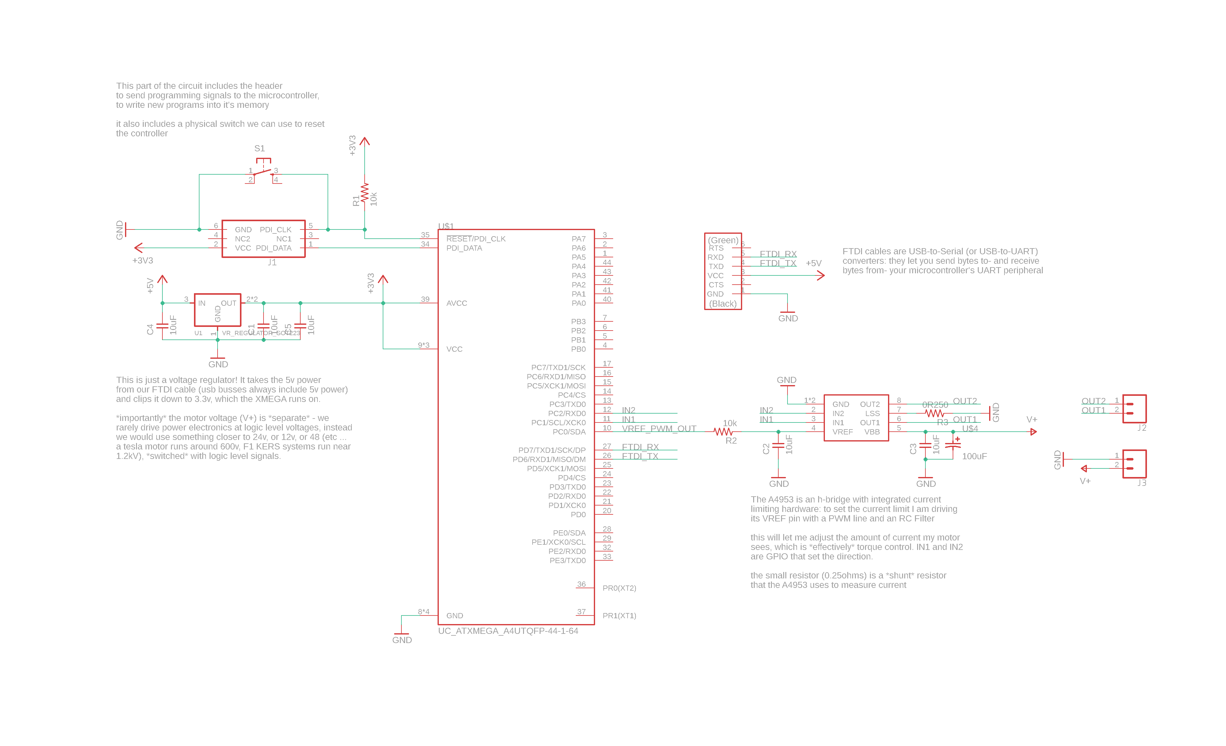
Critically, we can connect nets to one another by simply assigning them the same name. This is a useful trick that you will probably encounter many times in the wild. Also important to note are supply components, like the gnd and v+ or +3v3 etc symbols, which are simply symbolic representations of similarely named nets.
It's not-not useful to recall that schematics are also nice visual diagrams of what we want our circuits to do. There's no harm in making them look medium-nice. :bowtie:
The board representation is where our design meets the physical world. Here we find footprints that have pads that are connected to one another via traces, vias, and pours i.e. copper.
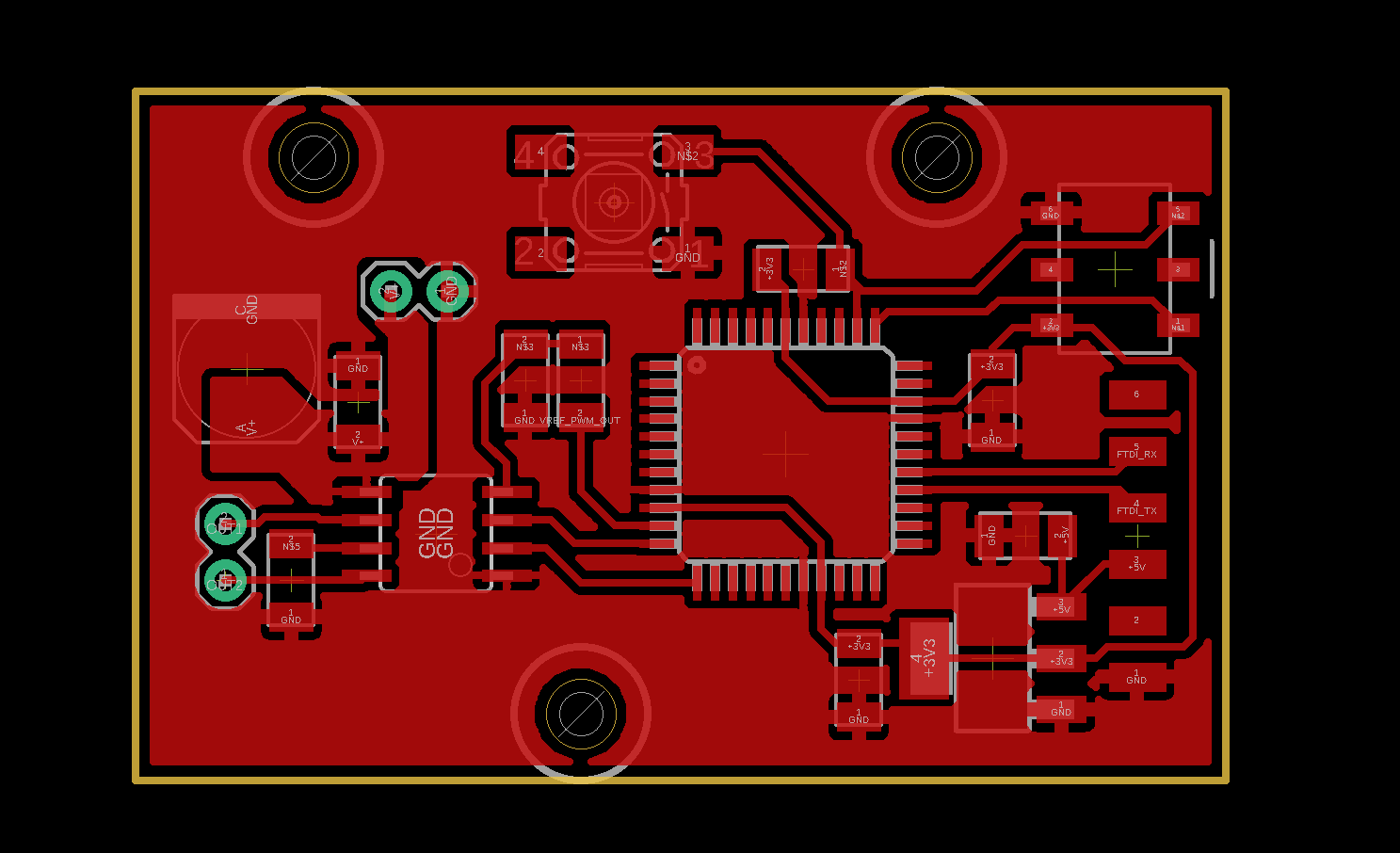
In Eagle, boards and schematics should be automatically associated with one another. This is referred to as 'forward/back annotation' - but typically goes one way: from the schematic to the board. It's best, while we're starting, to treat this relationship as a directional one. I.E. when you're deleting a component, do so in the schematic, otherwise you will introduce inconsistencies and Eagle might abandon you.
KiCAD uses a different system, where we save a netlist from our schematic, and open that in a board editor. This is partially an opinion about the division between the two practices, and partially a historic artefact of KiCAD's development as a collection of not-unrelated softwares.
Symbols and Footprints
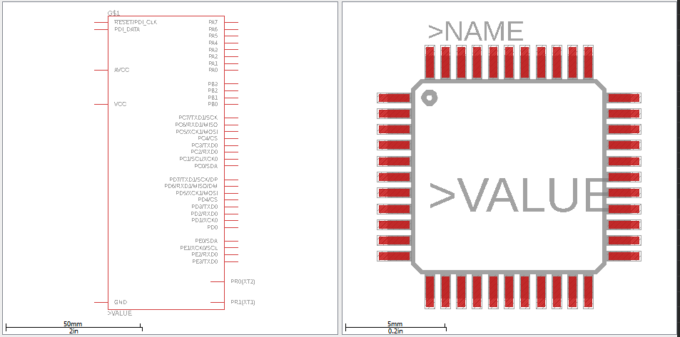
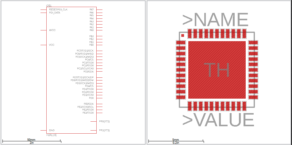
Our circuit assemblies are made of schematics that are diagrams of our boards, and so the components we use to put them together have a similar split; we call them symbols and footprints.
A symbol is a diagram of a part, and the footprint is the 'landing' that we need in order for the part to be successfully included in our circuit. The matching copper for us to hook the IC to.

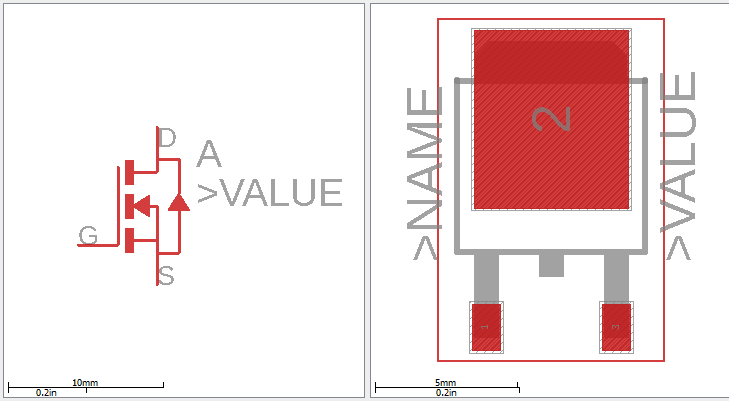
Symbols can have multiple footprints: the same or similar silicon divices can be packaged in varying sizes for circuit integration.